On November 29, the first CFCF2024 Asia-Pacific Optical Connectivity Forum, jointly organized by Fiber Optics Online and FNCA Asia-Pacific Fiber Optic Network Committee, was successfully held in Bangkok, Thailand. The conference focused on the optical communication supply chain and advanced packaging technology in Southeast Asia, and discussed topics such as industry development trends, supply and demand models, and technological innovation.

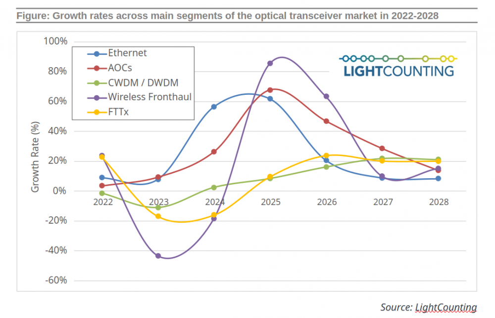
In the era of Artificial Intelligence (AI), stringent traceability of the origin of products offers unprecedented opportunities for manufacturing in Southeast Asia. With the surge in demand for cloud computing and AI, optical communication manufacturing is migrating to Southeast Asia, dominating the data center high-speed optical module market. According to Light Counting forecast, the global data center optical modules market is expected to reach USD 7.33 billion by 2025, growing at a CAGR of 14% from 2021 to 2025.

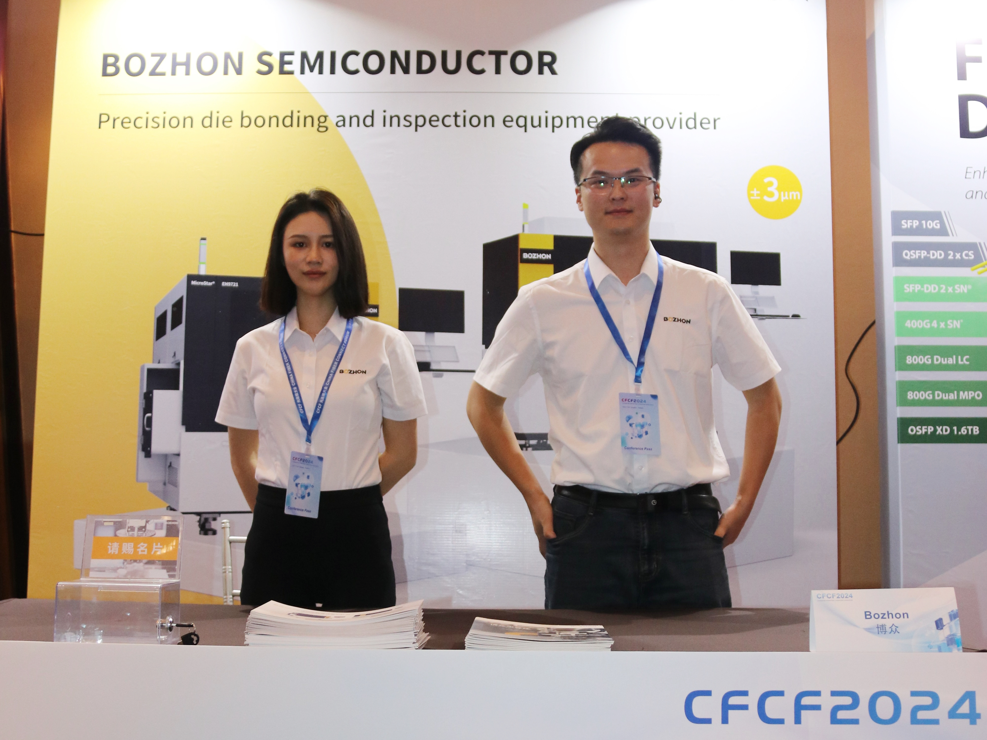
On the day of the forum, Bozhon Semiconductor was invited to attend the forum and provided perfect product consulting services to local customers and attendees through on-site staff explanation and face-to-face communication. Highlighting the high precision placement solutions for 800G/1.6T optical modules, the company realizes the placement needs of different designs, materials and process chips through COB, COC, COS, BOX and other packaging processes to meet the key challenges of higher speed rate and lower power data transmission of optical modules.

With the evolution of optical communications towards 800G/1.6T direction, the precision of optoelectronic device placement packaging from the traditional ± 7μm - ± 10μm to the current ± 3μm - ± 5um high-precision upgrades, the core driver of this change is that, with the miniaturization of the optical device and the integration degree of the continuous enhancement of the stability of the chip placement has become a key factor affecting the subsequent packaging process and device yields. In addition, the diversified needs of the optical module market have also exacerbated this challenge, and different customers often have their own unique placement process requirements, which puts forward higher requirements for automation equipment manufacturers to flexibly adapt to the ability.
In order to cope with this challenge, Bozhon Semiconductor launched the MicroStar series of eutectic die bonding adopts an innovative modular layout design, the core of this design strategy lies in the flexible combination of modular components, which can realize a rapid response to different process requirements and accurately meet the needs of the EH9722 eutectic mounter, as a new product launched by Bozhong Semiconductor, adheres to the integrated design of hardware and software to ensure that the ± 3um As a new product launched by Bozhon Semiconductor, EH9722 Eutectic die bonder adheres to the integrated design of hardware and software, which guarantees ±3um of mounter precision, and is equipped with a variety of mounter processes such as eutectic, dipping, dispensing, UV curing, etc., and the mounter depth of deep cavity can reach up to 17mm, which demonstrates its excellent ability in high-precision, intelligent and modular design.
Innovative Mechanical Structure Design
EH9722 eutectic die bonder adopts nanometer absolute double feedback gantry structure, and its unique horizontal turret mounter head design can manipulate 12 different nozzle tools at the same time and realize quick change of nozzle tools in motion to minimize the changeover time between different materials, processes and products. It is also equipped with multiple transit tables to meet customers' multi-chip and multi-process application scenarios, realizing one kind of equipment to meet the needs of multiple chip attachments, maximizing equipment utilization and reducing customers' operating costs.
Intelligent calibration and data software management system
Not only that, EH9722 eutectic diebonder is also equipped with advanced intelligent calibration system, which can automatically adjust the various parameters of the equipment to ensure the precision and stability of the mounter process. Meanwhile, the equipment's high-definition display process observation system can monitor every detail of the placement process in real time, providing strong support for the optimization of the production process. This intelligent management not only improves the production efficiency, but also reduces the risk of error caused by human operation. In addition, the equipment's self-developed eutectic friction process programming system can be customized according to the actual needs of the friction action, effectively reducing the placement of the void rate. This customization capability makes the EH9722 eutectic die bonder perfectly suited for a variety of optical module placement scenarios, providing users with efficient, stable and reliable placement solutions.
At present, Bozhon Semiconductor equipment has left its footprints in many countries and regions around the world, and has become one of the few Chinese brands in the semiconductor field capable of exporting its equipment in overseas regions by virtue of its excellent globalization sales, operation and service capabilities.
In the future, Bozhon Semiconductor will continue to maintain its technological advantages, and with its professional service capability, continue to create value for its customers, provide global customers with higher quality and higher performance placement equipment and full-scene placement solutions, and boost the industry's rapid development.


