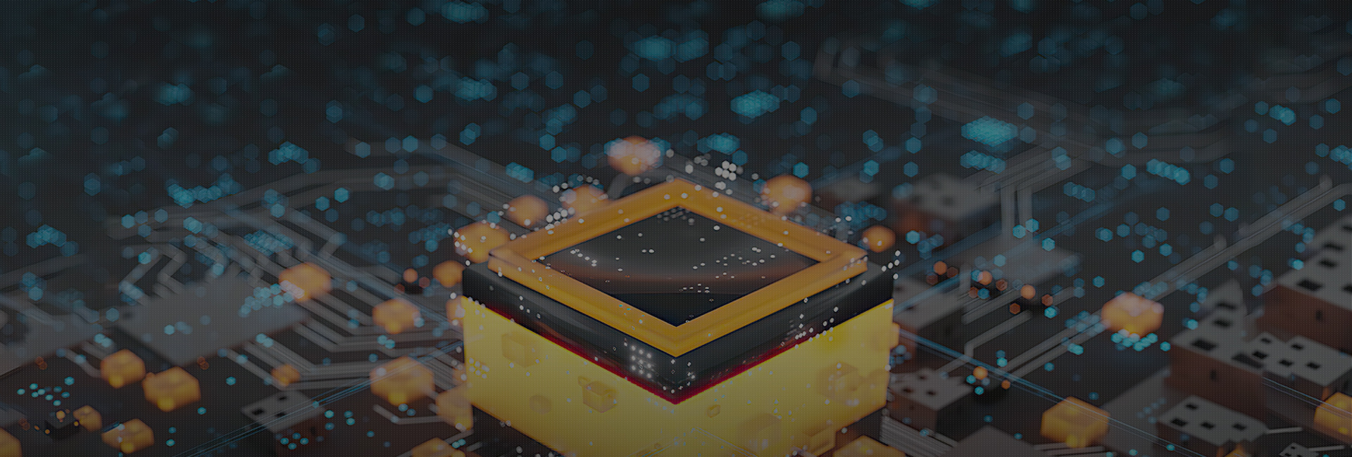
Semiconductor Inspection
Semiconductor Inspection
According to the link in the testing process, IC testing can be divided into design verification, front track measurement and back track detection. From the perspective of technical route principle, detection and measurement mainly include optical detection technology, electron beam detection technology and X-ray measurement technology, of which optical detection technology occupies a relatively large space.
The Challenge
With the continuous development of the manufacturing industry and the improvement of product fineness, AOI optical inspection equipment needs to have higher accuracy and faster speed to meet the high efficiency and high precision inspection needs on the production line. With the development of artificial intelligence, machine learning and other technologies, AOI inspection equipment will be more intelligent, and can continuously improve the accuracy and stability of detection through self-learning and upgrading, while reducing the false detection and missed detection rate. In the future, it is believed that AOI inspection equipment will be further integrated, integrating a variety of testing technologies into one device, achieving multi-angle and multi-level testing, and improving the comprehensiveness and accuracy of testing.


Our Recommendation
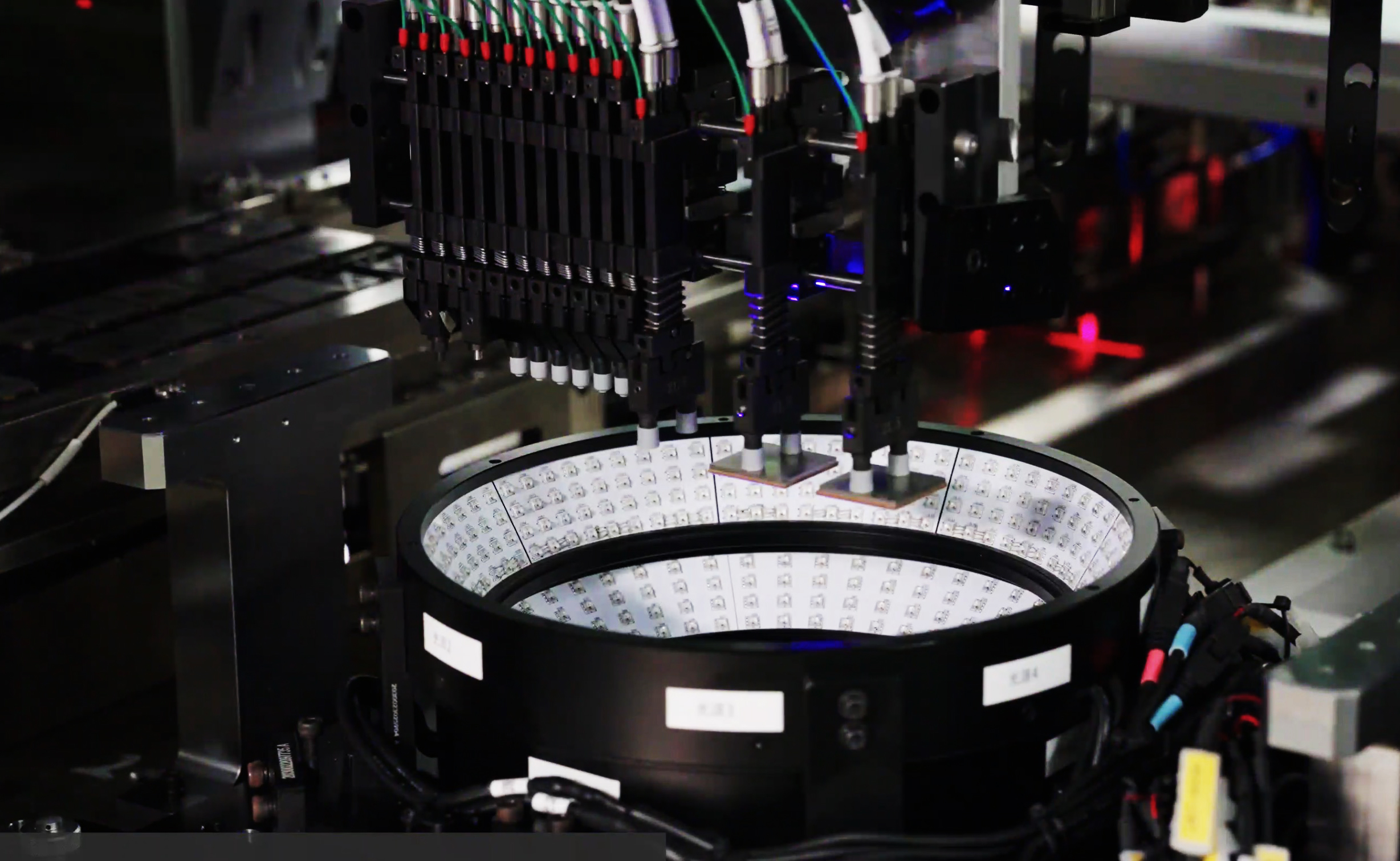
For BGA,LGA,QFN,QFP and other package chips, the CesiStar series TV6-15T provides comprehensive 6-side inspection and 2D/3D measurement to ensure the final chip package appearance quality and yield improvement. Compared with traditional 2D AOI, 3D AOI technology can perform stereoscopic inspection of electronic products in a fast and accurate way by using dedicated 3D sensors and camera systems. It can capture three-dimensional structure and appearance information to achieve comprehensive inspection of chips or other electronic parts.

Application Results
These configuration options make the CesiStar Series TV6-15T AOI inspection machine a complete assembly solution.

High precision
3D accuracy: ± 7.5μm@3σ; Supports 100μm BGA Balls; Support Surface dent detection; Support color detection

Ease of use
Fast change time

High compatibility
Compatible with BGA,QFN,LGA,QFP,SOP and other packaging forms; Covers 3*3mm-50*50mm chip sizes

Intelligent classification
Defect intelligent classification, 3 NG Buffer track
Related products