0512-63414949-80512
Service hotline

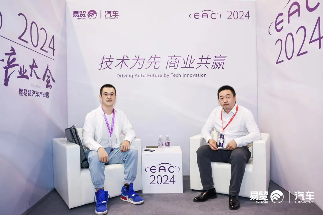
Recently, the EAC2024 E-commerce Automotive Industry Conference and Exhibition was grandly held at the Suzhou International Expo Center. This exhibition focuses on three major fields: new energy, intelligent driving, interior and exterior decoration, and intelligent cockpit. It consists of 30 forums, 7 exhibition areas, and more than 20 industry activities during the same period. XinShiye interviewed several excellent enterprises in the domestic automotive electronics industry chain and launched special reports.
This article is a transcript of XinShiye's exclusive interview with Fu Jiangbo, R&D Director of Suzhou Bozhon Semiconductor Co., Ltd. (hereinafter referred to as Bozhon Semiconductor).
Suzhou Bozhon Semiconductor Co., Ltd. is a direct subsidiary of Bozhon Precision Technology Co., Ltd., relying on Bozhon Precision Technology's more than 20 years of technological accumulation and focusing on semiconductors. And through industry university research cooperation with well-known domestic universities such as Tsinghua University and Harbin Institute of Technology, we provide high-precision, high-speed, and stable semiconductor die bonding equipment that meets advanced packaging requirements for customers in fields such as AI and optical communication, as well as efficient chip AOI detection equipment.

Against the backdrop of a large demand for ultra high speed optical modules, what challenges do optical module manufacturing face?
The demand for ultra high speed optical modules, as the core component of data transmission, is increasing in fields such as data centers, 5G communication, and high-speed internet. However, with the surge in demand, the optical module manufacturing industry is also facing unprecedented challenges.
From a technical perspective, high-speed evolution is one of the core challenges in the current optical module industry. With the increasing demand for bandwidth in data centers, the speed of optical modules is developing towards higher rates such as 800G or even 1.6T. The high precision and reliability of device packaging are crucial, which not only requires innovation in the design and manufacturing of optoelectronic devices, but also requires synchronous progress in material science and manufacturing processes.
The issue of heat dissipation is also one of the bottlenecks restricting the development of optical module technology. The high-speed operation of optical modules generates a large amount of heat. How to effectively dissipate heat and ensure the stable operation of the module is an important factor that must be considered in the design.
From the perspective of the supply chain, the management of the supply chain and cost control are also issues that manufacturers cannot ignore. With the development of optical modules towards higher rates, the required high-end materials and precision processes have led to rising costs. How to effectively control costs while maintaining competitiveness is also a challenge that manufacturers need to solve.
Compared to data centers and industrial applications, do automotive grade optical modules have higher packaging requirements, mainly reflected in which aspects?
There are certain differences and commonalities in packaging between data center optical modules and vehicle grade optical modules. Data center optical modules typically focus on high bandwidth, high-speed transmission, and low power consumption, adopting miniaturized and intensive packaging designs to adapt to high-density server racks and switch environments. The packaging of automotive grade optical modules needs to meet the special requirements of the automotive electronics field to ensure reliability, stability, and high performance in the vehicle environment. In automotive grade chip packaging, in addition to the requirements of high reliability, high precision, high heat dissipation, and small size, other technologies and considerations may also be involved, such as overcoming technical difficulties such as structural stress matching, water vapor isolation and sealing, high-strength aging resistance, ion migration, and optimizing heat dissipation efficiency, power density, vibration resistance, and temperature range adaptation.
The packaging schemes for different automotive grade optical modules may vary, and the specific packaging method will be selected and optimized based on factors such as the application scenario, performance requirements, and cost of the optical module. Meanwhile, with the continuous development of technology, the packaging of automotive grade optical modules is also constantly evolving and innovating to meet the development needs of automotive intelligence and networking. However, both have commonalities in pursuing high performance, low latency, and cost-effectiveness, requiring high-precision SMT equipment and packaging technology to improve overall performance and reliability. The optical module industry is highly collaborative with LiDAR, and supporting production facilities can be shared. Given the similarity between LiDAR and optical modules in terms of transmission and reception modules, optical module industry chain companies can reuse the advantages accumulated in technology, processes, supply chain procurement scale, and production capacity in this field for LiDAR business.
I see that Bozhon Semiconductor is focusing on the international market, and which regions are it mainly focusing on? How is the current progress?
We have learned that in addition to the traditional North American and European markets, optical module companies are gradually shifting their industries to emerging markets such as Southeast Asia, South Asia, and Africa. Southeast Asia, as an important global electronic product manufacturing base in the future, has nearly 80 optical communication companies of different scales setting up factories or offices here according to incomplete statistics.

What are the main pain points in the current manufacturing of optical communication modules? How can Bozhon solve it?
The rapid development of optical modules cannot be separated from the coordinated promotion of upstream and downstream industrial chains. This includes the joint efforts of manufacturers of optical devices, optical chips, electrical chips, and structural components, as well as packaging and testing equipment suppliers. Only close collaboration among various links in the industrial chain can ensure the sustainable development of the optical module industry.
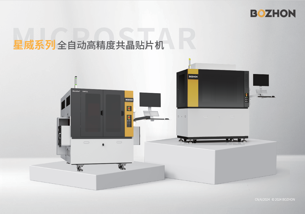
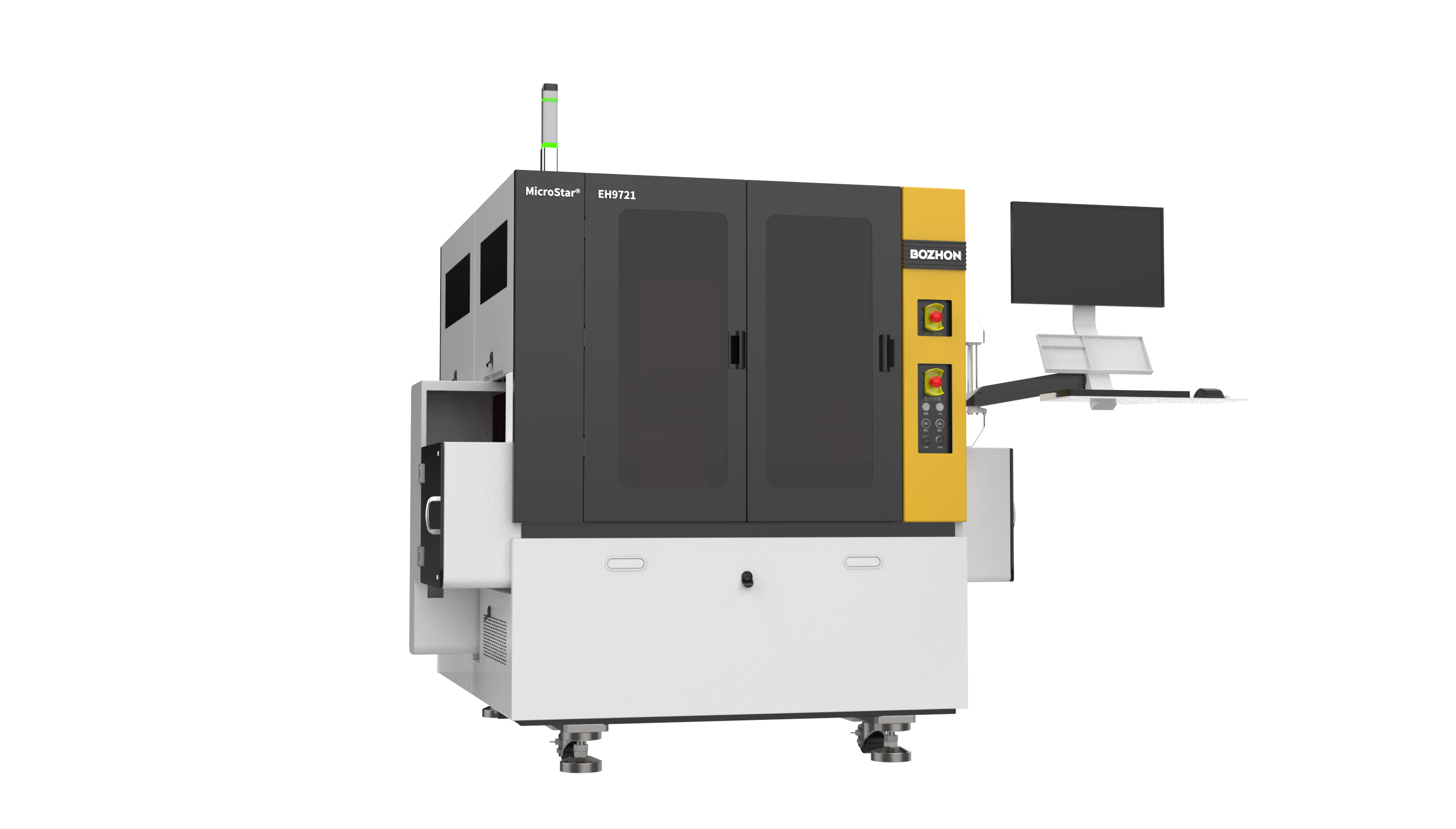
In the context of massive demand for ultra high speed optical modules, the manufacturing cost and process improvement of optical modules face extremely high technical challenges. It is necessary to use high-precision, high stability, and high flexibility automated process equipment to ensure that the produced high cost-effective optical modules have consistency, stability, and reliability, promote the vigorous development of the optical communication industry, and meet the needs of the artificial intelligence era. The EH9721 series fully automatic high-precision eutectic SMT machine from Bozhong Semiconductor is an ideal equipment for packaging optoelectronic devices and optical modules. This equipment combines eutectic SMT, dipping SMT, and Flip Chip SMT functions, and can meet the requirements of multi chip and multi process mounting scenarios. Advanced design and high-quality driving structure enable its mounting accuracy to reach ± 3 μ m, which can meet the high-density mounting requirements of single chip and multi chip optical modules. It is compatible with various packaging processes such as CoC, CoB, and CoS, and can be equipped with special functions such as UV heating, gluing, and screwing according to customer needs. It is worth mentioning that this series of equipment has undergone multiple technological upgrades and iterations, and currently has key technology layouts such as head heating, large-sized eutectic stage, and high-precision closed-loop force control. It can reduce the impact of thermal and mechanical stress on the performance of laser chips through an efficient and reliable eutectic heating system, and the high-precision closed-loop force control ZR module is more suitable for the bonding of high aspect ratio laser chips.
What are the new packaging requirements for 800G/1.6T optical modules compared to 400G optical modules?
Compared to 400G optical modules, 800G and 1.6T optical modules require higher signal integrity and lower power consumption, which requires packaging technology to effectively reduce signal loss and heat accumulation. Specifically, 800G/1.6T optical modules typically have the following packaging requirements:
Higher precision: With the continuous iteration and upgrading of optical modules, higher assembly accuracy is required and higher precision equipment is needed. For example, using CPO technology to place optical communication components and electronic chips in the same package can achieve shorter signal transmission paths and higher performance.
High integration: For example, silicon optical modules highly integrate lasers, modulators, and detectors onto silicon optical chips, while effectively controlling power consumption. This helps to reduce packaging volume, improve module density and performance.
Low cost: By improving integration, packaging costs can be reduced, and silicon-based materials can be manufactured in large sizes, which also helps to reduce the cost of silicon-based chips.
Process simplification: By using compatible and mature CMOS processes, the packaging process can be simplified. When upgrading to 800G and 1.6T, compared to the significantly increased process steps of traditional optical modules, silicon optical chips only need to design a few more channels, and the process changes are relatively small.
In addition, 800G and 1.6T optical modules also have higher requirements for materials and processes. Packaging materials need to have better thermal conductivity and electrical insulation performance to cope with the heat dissipation and electrical isolation challenges brought about by high power density.
Can you share the current commercial progress of 800G optical modules?
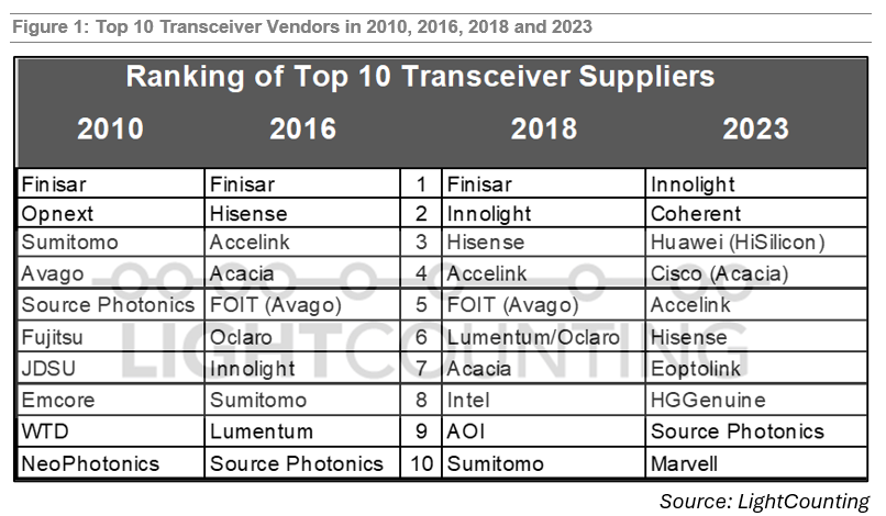
The explosion of AI demand is accelerating the layout of 800G optical modules. It is reported that since 2023, major North American customers have started large-scale procurement, especially the newly added AI major customer Nvidia, which has brought new impetus to performance growth and confirmed the strong demand for 800G upgrades. The competitive landscape in the industry is relatively stable, and leading manufacturers continue to lead the development of the industry. According to LightCounting's 2023 Global Top 10 list of optical modules, a total of 7 Chinese optical module manufacturers have been shortlisted, including Xuchuang Technology (ranked 1st), Huawei (ranked 3rd), Guangxun Technology (ranked 5th), Hisense Broadband (ranked 6th), Xinyi Sheng (ranked 7th), Huagong Zhengyuan (ranked 8th), and Sols Optoelectronics (ranked 9th). This also confirms the technological breakthroughs of Chinese manufacturers in the field of high-end optical modules and the trend of domestic substitution.
The commercial use of 800G optical modules cannot be achieved without innovation and maturity in the industrial chain. At present, Bozhon Semiconductor's eutectic mounting machine equipment has the ability to install 800G optical modules with high precision. In the future, our products will continue to innovate and iterate, develop together with the industry, and continue to empower the research and implementation of higher speed optical module mounting solutions such as 1.6T and even 3.2T.
What are the technical difficulties of optoelectronic co packaging (CPO)? Will it overturn traditional technology? Can we start a conversation.
Co packaged optics (CPO) technology adopts an innovative packaging method, which tightly packages optical modules and chips in the same packaging body, greatly reducing the connection length and distance between them.
Simply put, CPO is the process of continuously bringing optical modules closer to switching chips, shortening the wiring distance between chips and modules, and gradually replacing pluggable optical modules. Ultimately, the optical engine and electrical switching chips are packaged into one chip, which can reduce signal attenuation, system power consumption, and achieve high integration. CPO technology is currently in the early stages of industrialization, and although it has enormous potential, it still faces a series of key technical problems that urgently need to be solved.
CPO faces severe technical challenges in various aspects such as process, simulation, and testing. Among them, packaging process capability is one of the key factors restricting the development of CPO technology. The packaging of CPO involves various advanced and complex packaging technologies such as TSV (silicon via) and TGV (glass via). These technologies each have their own advantages and disadvantages, and continuous exploration and optimization are needed in the research and manufacturing process to find the most reliable solutions. The development of CPO technology also faces multiple other challenges. For example, how to choose a suitable optical engine modulation scheme to ensure the accuracy and stability of data transmission; How to package the internal components of an optical engine to achieve efficient photoelectric conversion and signal transmission; And how to achieve feasible high coupling efficiency light source coupling in mass production to improve overall optical performance. In summary, CPO packaging technology not only brings about changes in device system architecture, but also requires new chip manufacturing and packaging automation solutions. Bozhong Semiconductor looks forward to leveraging its technological advantages in the future process of optoelectronic co packaging (CPO), working together with industry colleagues to promote technological innovation and development in the optoelectronic industry.
Does China occupy a dominant position in the SMT market? Do you think there is a lot of competitive pressure in this industry? Can we start a conversation.
The domestic SMT machine market has undergone a transformation from relying on imported brands to the rise of domestic technology. In the past, due to relatively backward technology, the domestic market was dominated by imported brands for a long time. In recent years, with the background of national policies, capacity transfer, and technological innovation, domestic manufacturers have caught up and gradually narrowed the technological gap with foreign countries. Not only has it occupied a place in the mid to low-end market, but it is also gradually entering the high-end market, demonstrating strong development momentum.
In competition, leaders often have more resources and advantages. Faced with the continuous development of the semiconductor high-end equipment industry, domestic equipment manufacturers will inevitably need to continue to overcome difficulties and innovate in research and development. Through continuous R&D investment, Bozhon Semiconductor has significantly narrowed the gap with international leading technologies. The MicroStar series eutectic die honding machines have achieved high-precision and long-term stable installation of 3 microns, and the key components of the equipment are independently developed. This not only effectively guarantees the supply of key components, but also allows for targeted development and design based on the overall performance requirements of the equipment, ensuring high performance and product competitiveness of the equipment. The product demonstrates greater flexibility and advantages in meeting personalized customer needs, and can provide customized and modular equipment structure design. To continuously meet the needs of industry development, Bozhon Semiconductor will combine its own industrial advantages, gradually expand the research and development of advanced packaging equipment on the basis of continuously cultivating high-precision eutectic die bonding machines, and combine the automation integration advantages of Bozhon Group to meet the high-speed development of the industry.