0512-63414949-80512
Service hotline

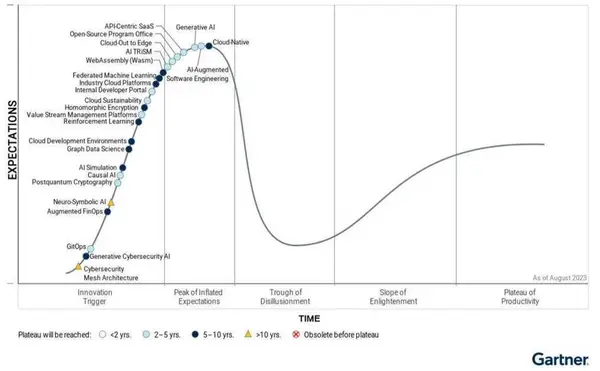
Driven by the global wave of digitisation and intelligence, Artificial Intelligence (AI) technology is growing at an unprecedented rate. According to market research firm Gartner, the AI chip market has shown explosive growth over the past few years. According to forecasts, the global AI semiconductor market size is expected to grow by 25.6 per cent to reach $67.1 billion in 2024 and is expected to continue to grow at a high rate in the coming years. By 2027, the market size is expected to reach $119.4 billion, growing at a CAGR of over 30%.
Trends ▹ Growing Demand for AI Chips
The rapid growth of AI chips is attributed to the widespread application of AI technology in various industries, such as autonomous driving, intelligent manufacturing, and healthcare, etc. The continuous improvement of AI algorithms and computational capabilities has led to a sharp increase in the demand for high-performance AI chips, and the explosive growth in the volume of data has further pushed up the demand for more efficient data processing and analysis.
Generative AI , as an important branch of AI technology, has demonstrated strong capabilities in the generation and processing of multimodal data such as images, text, and audio. Generative AI has a wide range of applications, from content creation, virtual reality, game development to medical image generation, etc., and various fields have put forward higher demand for AI chips. The pull of generative AI on chips is mainly reflected in the following aspects:
·Increased demand for computing power:Generative AI models, such as GPT-4 and DALL-E, usually require huge computational resources for training and inference. This places extremely high demands on the arithmetic power and efficiency of AI chips, driving the development and production of high-performance chips.
·Optimisation of energy efficiency ratio:The training and inference process of large-scale models in generative AI applications consumes a lot of energy. How to reduce energy consumption while increasing arithmetic power has become a key challenge in chip design and fabrication.
·Storage and bandwidth requirements:Generative AI handles huge amounts of data, which increases the storage and bandwidth requirements. This requires AI chips to have higher performance in terms of storage architecture and data transfer.
Manufacturing ▹ AI chip packaging process
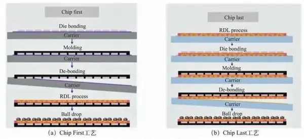
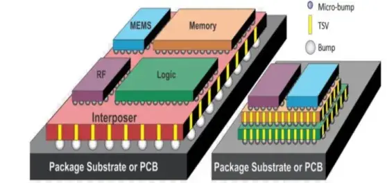
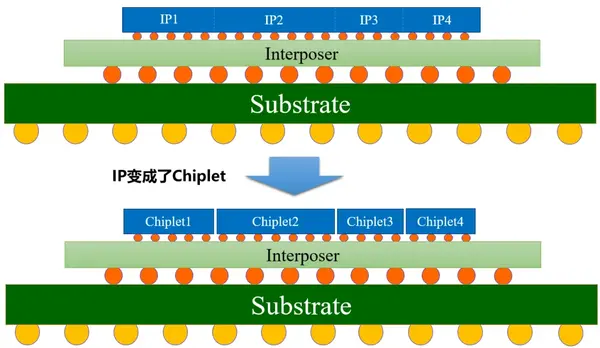
The process of AI chips is both complex and rigorous, with arithmetic power and power consumption being the two key indicators of their performance. In the post-Moore era, increasing arithmetic power and reducing power consumption rely more and more on advanced packaging technologies, such as rewiring layers (RDLs), silicon via vias (TSVs), silicon intermediary layers, and microbumps. Currently, the major advanced packaging technologies include fan-out (FO) packages, 2.5D/3D packages and Chiplet technology.
◎ FO Packaging Technology
FO package connects the chip pads from the edge of the chip to the PCB through RDL and solder balls, thus increasing the available wiring area, making full use of the chip area, and reducing the cost. The advantage of FO package is that it does not need to cover the load board, directly soldered to the PCB, shortening the signal transmission distance and improving the electrical performance.FO package technology has been widely used in artificial intelligence, 5G communications, millimetre wave radar and other fields.
◎ 2.5D/3D Packaging Technology
3D integration technology achieves electrical interconnections between different chip layers through TSV, including 3D IC packaging, 3D IC integration and 3D Si integration. 3D-IC packaging can accommodate multiple heterogeneous dies, and each functional module can use different process nodes, reducing costs and speeding up time-to-market. 3D-IC technology supports smaller sizes, saves space, and is suitable for small mobile devices. The technology has a wide range of applications in CPUs, GPUs, smartphones, and high-performance computing, and is one of the effective paths to continue Moore's Law.
◎ Chiplet technology
Chiplet is a design concept whereby a complex SoC chip is dispersed into multiple dies with specific functions, and then integrated into a multi-functional heterogeneous SiP through packaging technology.Chiplet solutions offer higher design yields and lower costs compared to traditional single-chip solutions. Studies have shown that when the chip area is large, the yield of the Chiplet solution is significantly higher than that of a single chip solution.Chiplet technology also allows for the connection of chip packages in different processes, which improves packaging flexibility, enhances the utilisation of advanced processes, and reduces costs.
Empowering ▹ High-precision placement solutions to boost productivity
At the same time, the complex operating environment also has strict requirements for the stability and reliability of AI chips. High-precision solid crystal machine equipment plays a crucial role, in which precision, speed and stability are the most core indicators. Products and mounting solutions from Broadchoice Semiconductor can provide manufacturers with high-precision solid crystal and eutectic placement processes, helping them to produce high-performance AI chips.
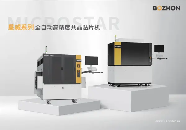
Bozhon Semiconductor high-precision eutrctic die bonding precision up to 0.5-3μm, both multi-head mounting capabilities, can simultaneously deal with a variety of chip placement, improve production efficiency, to meet the needs of large-scale mass production. It is worth mentioning that the AI chip chip placement eutectic process needs to be carried out at high temperatures, MicroStar series eutectic machine with good temperature control capabilities, heating only 3.2s, cooling only 6.5s, can maintain a stable temperature environment throughout the entire process, to ensure uniform melting of the solder and reliable chip placement. And the whole machine adopts modular design, with a high degree of flexibility, can be adapted to different sizes and types of chips to meet diversified production needs.
In the future, we can foresee that with the further development and innovation of high-precision eutectic machine technology, the manufacturing of AI chips will become more precise and efficient. This will not only promote the intelligent transformation of various industries, but also bring more convenience and possibilities to our lives.